
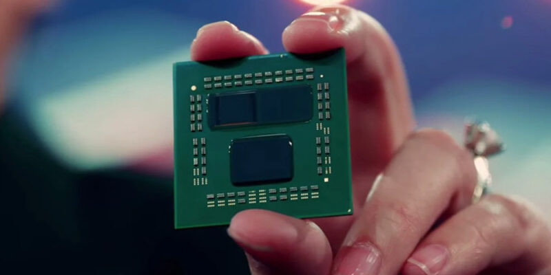
Semiconductor manufacturing demands an unprecedented level of precision, with features now measured at the atomic scale. Traditional inspection methods are no longer sufficient to detect the smallest defects that can impact chip performance. Erik Hosler, a leading expert in advanced metrology and process optimization, recognizes that optical metrology innovations are transforming semiconductor inspection, enabling higher accuracy, faster detection and improved yield.
The Evolution of Optical Metrology in Semiconductor Manufacturing
Optical metrology has long been a cornerstone of semiconductor inspection, but recent innovations are expanding its capabilities. Today’s advanced tools leverage high-resolution imaging, interferometry and AI-driven analysis to provide real-time feedback and minimize process variability.
Modern optical inspection systems excel in:
Defect detection: Identifying nanoscale defects that traditional techniques might miss
Process optimization: Enhancing lithography accuracy by refining pattern alignment
Non-destructive analysis: Reducing waste by inspecting wafers without physical contact
These advancements ensure that chipmakers can meet the demands of cutting-edge semiconductor technologies, from AI processors to 3D-stacked devices.
High-Harmonic Generation and Free-Electron Lasers: Pushing the Boundaries
New light sources are redefining what’s possible in semiconductor inspection. Free-electron lasers will revolutionize defect detection by offering unprecedented accuracy at the sub-nanometer scale, notes Erik Hosler. These lasers generate high-intensity, tunable wavelengths that penetrate deeper into semiconductor materials, revealing defects hidden within multi-layer chip structures.
Similarly, high-harmonic generation (HHG) sources are improving resolution in extreme ultraviolet (EUV) lithography inspections, allowing fabs to identify variations at the atomic level. This level of precision is critical as chip features shrink beyond traditional metrology limits.
AI-Powered Optical Metrology: Smarter, Faster, More Reliable
Artificial intelligence is now an integral part of optical metrology, improving defect classification and measurement accuracy. AI-driven tools can:
Analyze complex patterns and detect inconsistencies at a scale too fine for human inspection.
Automate defect categorization, reducing human error and accelerating decision-making.
Predict process deviations before they cause defects, optimizing yield and efficiency.
By integrating AI with optical metrology, fabs can reduce false positives, optimize inspection workflows and minimize costly production delays.
The Future of Semiconductor Inspection
With next-generation optical metrology tools, semiconductor manufacturers are achieving breakthroughs in defect detection and process control. These innovations not only ensure higher yields but also pave the way for even smaller, more powerful chips.
As semiconductor scaling continues, advanced optical metrology will ensure quality, reliability and efficiency—key factors in driving the industry’s next wave of technological advancements.


Comments